Organic photovoltaics (OPVs) are emerging as a promising class of solar technology thanks to their lightweight nature, mechanical flexibility, and compatibility with low-cost, solution-based manufacturing. These features make them ideal for applications ranging from building-integrated photovoltaics [1] to portable and indoor power sources [2]. However, achieving both high performance and long-term stability remains a key challenge as the field moves from laboratory-scale devices toward real-world deployment.
The performance of OPV devices is closely tied to the internal organization of their active layers. These layers typically consist of a blend of electron-donating and electron-accepting organic semiconductors. The nanoscale morphology of these materials (their packing, orientation, and phase separation) determines how effectively sunlight can be converted into electrical current [3]. Consequently, understanding and controlling this structure is critical for improving both efficiency and operational durability.
Two common approaches exist for depositing the active layer in OPVs: bulk heterojunction (BHJ) and layer-by-layer (LBL) fabrication [3, 4]. In BHJ devices, the donor and acceptor materials are mixed together in solution and coated simultaneously. This method is straightforward and often yields high initial performance, but the resulting morphology can be difficult to control and may evolve under thermal or light stress. In contrast, the LBL approach sequentially deposits the donor and acceptor layers, offering greater control over molecular organization. While more complex to implement, this method may offer enhanced structural stability.

Figure 1. (a) Conventional OPV device architecture using either bulk heterojunction (BHJ) or layer-by-layer (LBL) fabrication. In BHJ, the donor (PM6) and acceptor (Y7-12) are blended; in LBL, they are deposited sequentially. PEDOT:PSS serves as the hole transport layer (HTL), and ZnO as the electron transport layer (ETL). (b) Inverted architecture devices using the same BHJ and LBL strategies, with reversed order of transport layers: ZnO is placed directly on the substrate as ETL, and BM-HTL is used under the silver electrode. (c) Schematic representation of the slot-die coating process, used to deposit each layer from solution under ambient air conditions. (d) Chemical structures of the donor polymer PM6 and the non-fullerene acceptor Y7-12, which together form the light-absorbing active layer. All devices were built on glass substrates coated with ITO (indium tin oxide), a transparent, conductive oxide that serves as the bottom electrode. Credit: APL Energy (2025), DOI: 10.1063/5.0270441
Scalable Fabrication Meets Structural Characterization
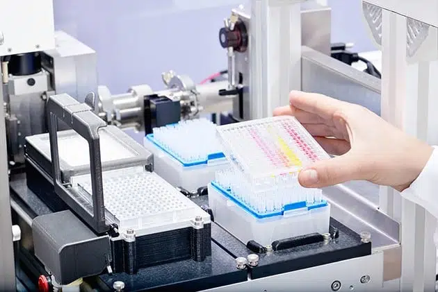
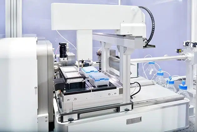
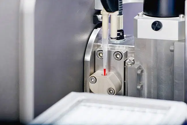
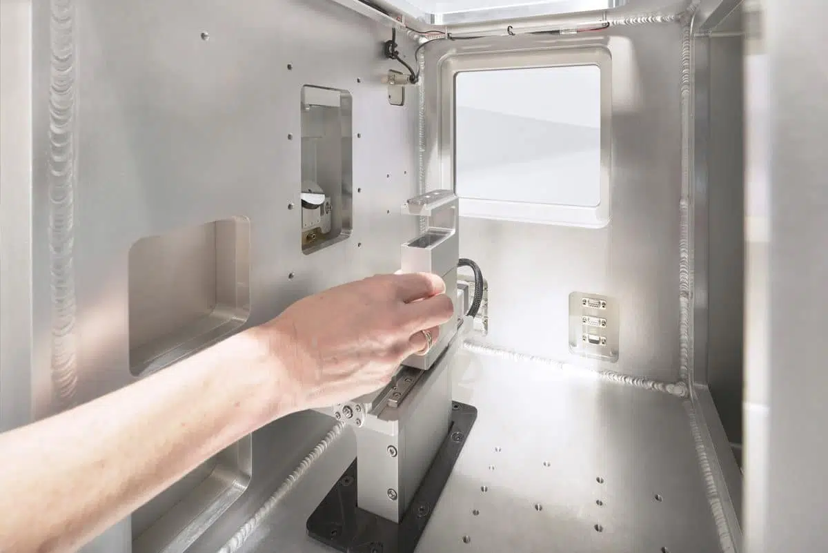
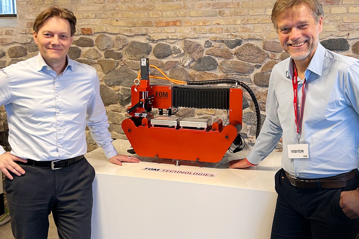
In a recent study researchers from the Technical University of Denmark and the University of Southern Denmark [5] explored how the BHJ and LBL fabrication strategies influence the efficiency and long-term stability of OPV devices. All active layers and interfacial coatings were deposited under ambient conditions using a FOM alphaSC slot-die coater from FOM Technologies, a system designed for scalable, reproducible film deposition. The donor material used was PM6, and the non-fullerene acceptor was Y7-12. Devices were constructed in both conventional and inverted architectures to evaluate the impact of structure and layer sequence on performance.
Initial power conversion efficiencies were high across all device types, with the best-performing BHJ device achieving 15.24% Power Conversion Efficiency (PCE). However, when exposed to prolonged thermal stress, some devices degraded more rapidly than others. To understand why, the team turned to grazing-incidence wide-angle X-ray scattering (GIWAXS), a technique ideally suited for probing the molecular ordering and crystalline domains in thin organic films.
What Did GIWAXS Reveal About Morphology?
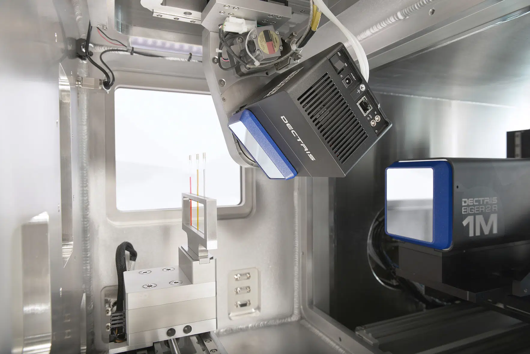
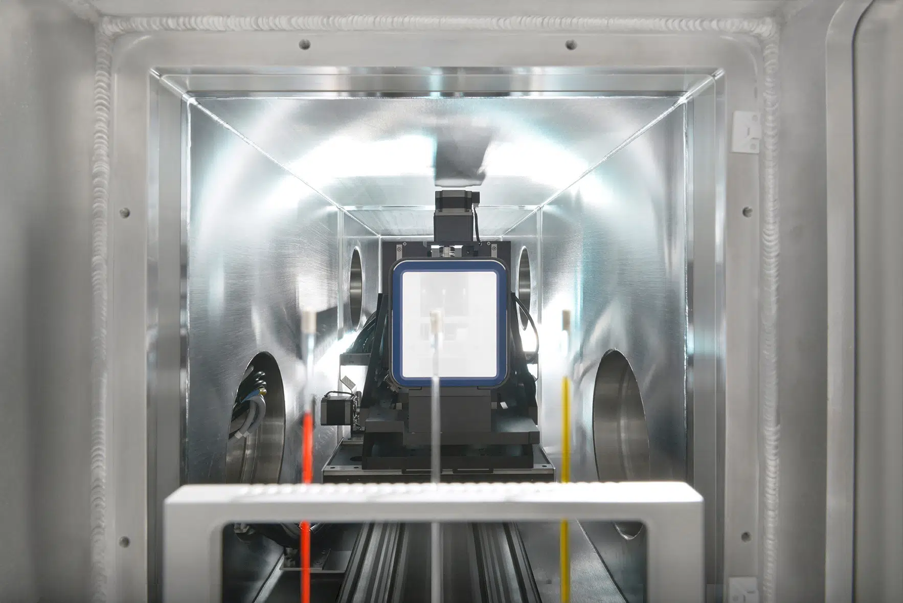
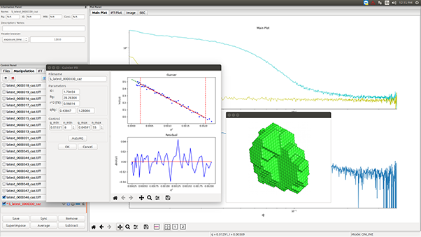
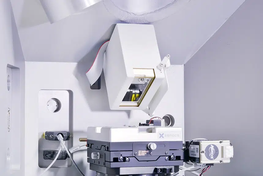
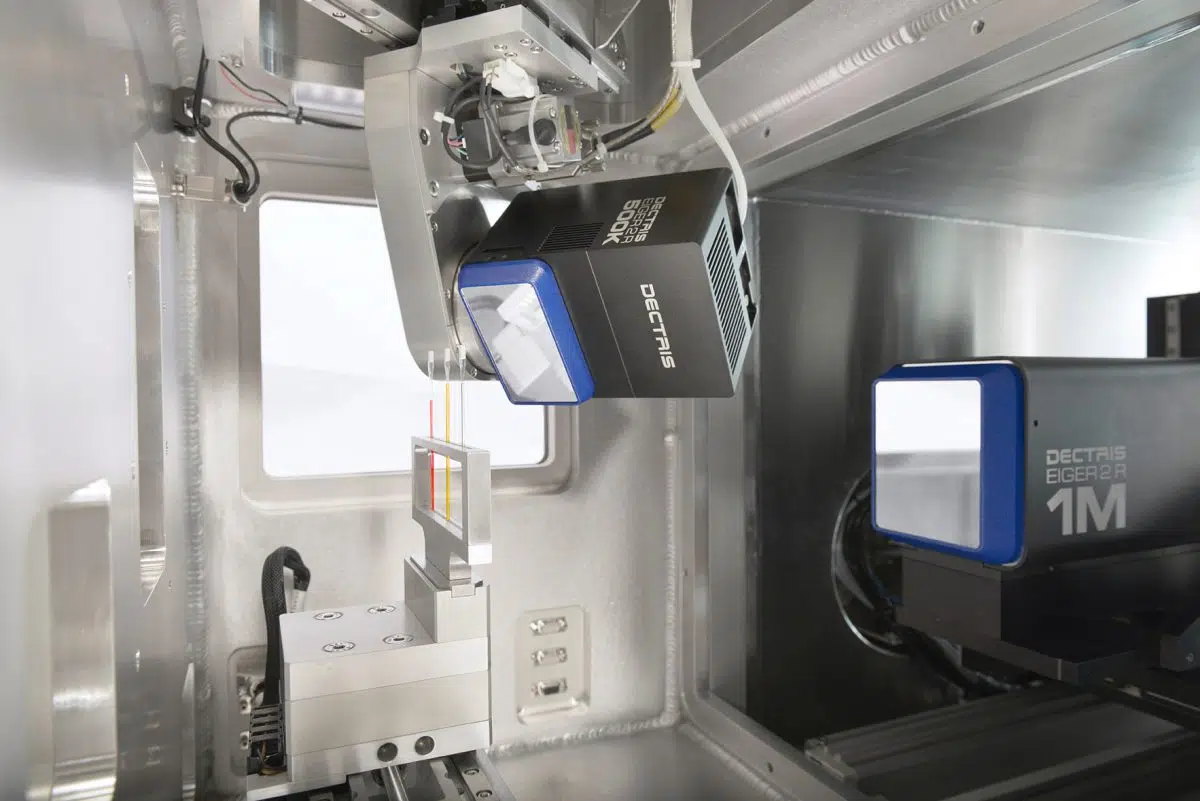
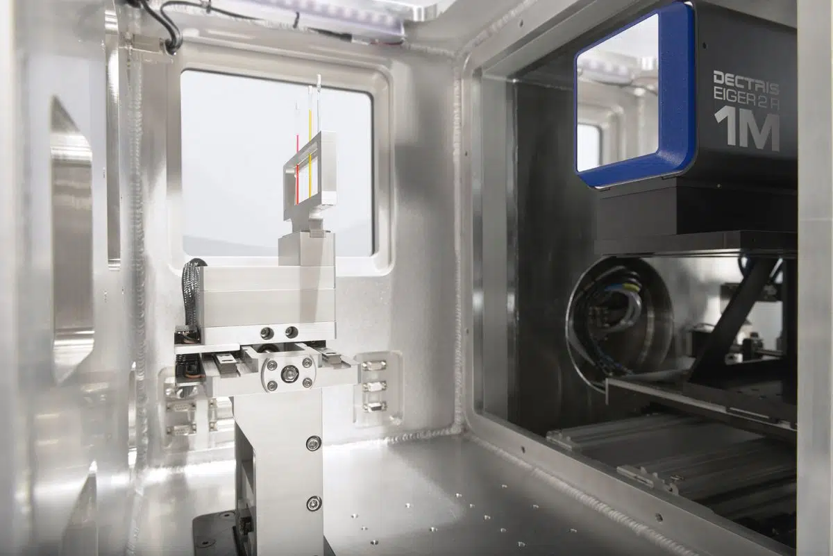
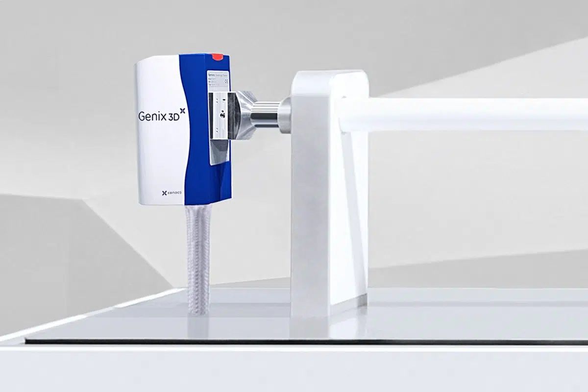
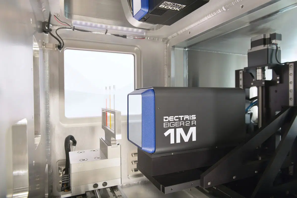
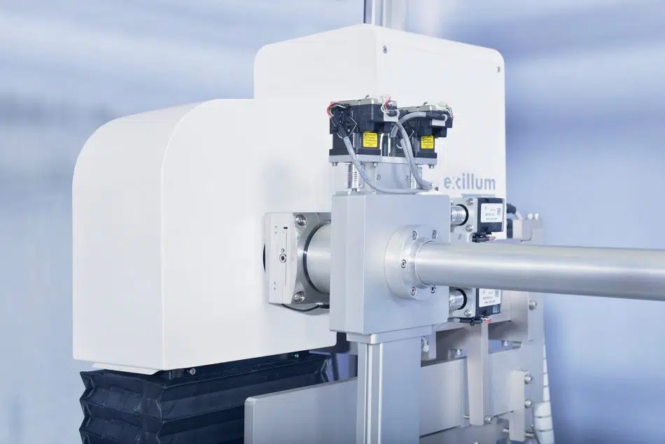
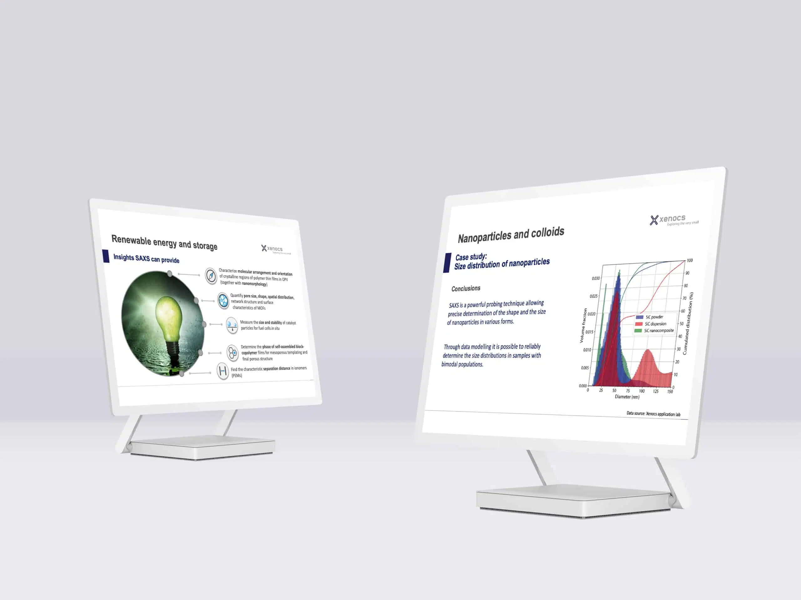
To assess the nanostructural stability of the active layer, the researchers performed GIWAXS measurements using a Xenocs Xeuss 3.0 system. These measurements were conducted on LBL PM6:Y7-12 films, which were spin-coated onto glass substrates for optimal film uniformity during analysis.
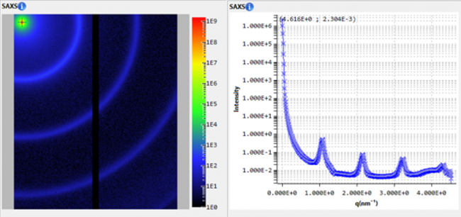
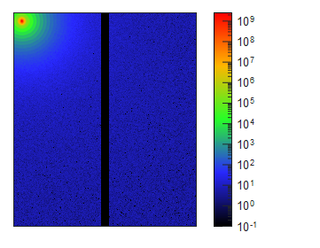
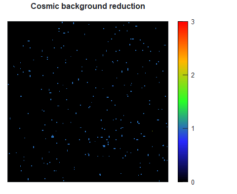
The 2D GIWAXS patterns collected before and after thermal aging revealed a clear lamellar diffraction peak at Q ≈ 0.3 Å⁻¹, corresponding to the PM6 polymer’s crystalline packing. Crucially, this peak remained unchanged even after 72 hours of thermal exposure at 85 °C, indicating that the bulk morphology of the photoactive layer was not significantly altered by thermal stress (Figure 2).
Further analysis of the 1D in-plane scattering profiles confirmed that no degradation-induced shift or broadening occurred. These results demonstrated that the nanoscale ordering of the active layer remained stable under prolonged thermal stress.

Figure 2. Structural characterization of the PM6:Y7-12 active layer using GIWAXS. (a) Two-dimensional GIWAXS pattern of the active layer, collected at a grazing incidence angle of 0.28° with an X-ray wavelength of 1.5418 Å. The scattering features in reciprocal space reveal the crystalline organization of the PM6 donor polymer within the blend. (b) In-plane line profiles extracted from the 2D GIWAXS patterns, comparing fresh and thermally aged films. The preservation of the lamellar diffraction peak at Q ≈ 0.3 Å⁻¹ after aging indicates that the molecular packing of the donor polymer remains stable under thermal stress. Credit: APL Energy (2025), DOI: 10.1063/5.0270441
Where Does Degradation Really Happen?
While the GIWAXS results ruled out morphological instability in the active layer, some devices—particularly conventional BHJ structures—still exhibited a decline in performance after thermal aging. This prompted the researchers to investigate other parts of the device stack.
By combining electrical measurements (such as EQE and J–V analysis) with optical microscopy and atomic force microscopy, they identified the interface between the top silver electrode and the adjacent hole transport layer (BM-HTL) as the likely site of degradation under thermal stress. Changes at this interface—such as delamination or morphological roughening—were shown to reduce fill factor (FF) and open-circuit voltage (Voc), even as the short-circuit current (Jsc) remained unaffected.
Thanks to the structural stability confirmed by GIWAXS, the team was able to confidently attribute the observed degradation to interfacial failure rather than bulk material instability. This insight is critical for guiding future improvements in OPV design, especially when it comes to selecting more stable interfacial layers or alternative electrode materials.
BHJ vs. LBL: Which Deposition Strategy Ensures Greater Stability?
The study found that both BHJ and LBL devices could achieve high efficiency under scalable processing. However, when subjected to thermal stress, inverted LBL devices consistently demonstrated superior stability. These devices maintained high performance with minimal decline over time—suggesting that the controlled morphology provided by LBL processing, combined with a more robust inverted architecture, offers a promising route toward durable, large-area OPV modules.
Why Structural Insights Matter for Scalable Solar Devices
This work underscores the power of using GIWAXS for evaluating device stability and guiding materials selection for the next generation organic solar cells. By combining scalable fabrication using FOM Technologies’ slot-die coating platform with high-resolution nanostructural analysis enabled by Xenocs’ advanced laboratory X-ray instrumentation, the researchers were able to directly link processing techniques, nanoscale organization, and long-term performance.
Their findings show that while high initial efficiency is important, understanding and controlling the molecular-level stability of OPV materials is essential for building reliable, commercially viable solar devices. By providing direct access to nanoscale structural features like molecular packing, crystallinity, and molecular orientation, GIWAXS enables researchers to decode how active layers organize during processing [3] and evolve under stress. These structural insights are essential for optimizing performance and ensuring the long-term stability of scalable organic solar devices.
The work presented here highlights the value of combining scalable fabrication techniques with advanced structural analysis to better understand and improve organic solar cell performance. To help researchers move even faster, Xenocs and FOM Technologies have launched a strategic partnership — with the goal of enabling in situ characterization during slot-die coating.