Surface Structure and Patterns by GISAXS/GIWAXS
The structure of surfaces and thin films plays a decisive role in technologies ranging from organic electronics and semiconducting devices to membranes, coatings, catalysis, and advanced nanofabrication. At these length scales, ordering and texture within the top layers of a material control charge transport, mechanical performance, chemical reactivity, permeability, and optical behavior.
Grazing-Incidence Small-Angle and Wide-Angle X-ray Scattering (GISAXS/GIWAXS) provide powerful, non-destructive tools to characterize surface and thin-film morphology. In particular, by probing the surface under grazing incidence, these techniques reveal in-plane and out-of-plane order, structural periodicities, orientation, and crystalline or nanostructured motifs with nanometer to sub-nanometer sensitivity.
What is measured?
Grazing-incidence X-ray scattering combines SAXS and WAXS in a geometry that enhances sensitivity to thin films and near-surface structures. The resulting 2D detector images contain complementary information about mesoscopic morphology (GISAXS) and crystalline structure (GIWAXS).
From these patterns, the techniques provide access to:
- Lateral and vertical periodicities, observed as characteristic scattering maxima or Bragg features that reflect long-range or medium-range order in the film
- Characteristic length scales, such as in-plane domain spacing, feature size, pore dimensions, or layer thicknesses, derived from the positions of small-angle scattering features
- Orientation and texture of nanostructures, obtained from the angular distribution of scattering intensity in the 2D pattern
- Crystalline packing within thin films, characterized by GIWAXS peak positions, shapes, and relative intensities, giving insight into unit cell parameters and crystal orientation
- In-plane versus out-of-plane correlations, revealed by the distribution of intensities along in-plane and out-of-plane directions, indicating anisotropy and preferred orientation in the film

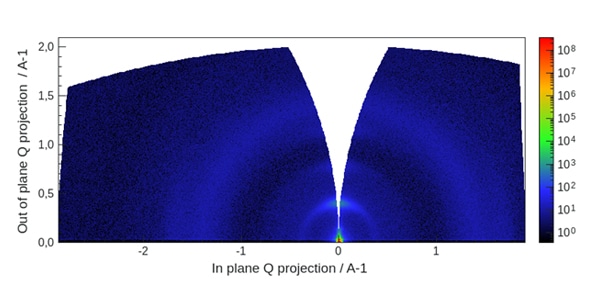
Figure 1. Wedge corrected grazing incidence wide angle x-ray scattering data acquired on a P3HT:PCBM thin film on a silicon substrate. processed with XSACT Pro to highlight in-plane and out-of-plane structural motifs.
Moreover, tructural parameters can be extracted either directly from the 2D scattering maps or from 1D cuts along selected directions (in-plane, out-of-plane, or along specific reciprocal-space paths), depending on the question and level of detail required.
Samples
GISAXS and GIWAXS apply broadly to thin films and surface-engineered materials whose structure is confined near the interface. For example, they are well suited for:
- Nanopatterned surfaces
- Nanostructured or porous thin films, including block-copolymer templated materials
- Layered or nanolamellar systems, such as polymer or inorganic multilayers
- Hybrid or inorganic thin films, including oxides, semiconductors, and sol–gel derived materials
- Organic electronic materials, such as conjugated polymers and donor–acceptor blends
Because the technique is non-destructive and requires no conductive coating or sectioning, researchers can analyze samples directly on substrates such as silicon, glass, metals, or flexible films.
Why use GISAXS/GIWAXS for Surface Structure and Pattern Analysis?
GISAXS and GIWAXS offer structural insight uniquely tailored to surface and thin-film materials:
Surface sensitivity by design
Selectively probing nanostructures within the top layers without damaging the sample.
Statistically representative measurements
Capturing morphology across large illuminated areas rather than limited local regions.
Applicability to conducting and non-conducting materials
Enabling broad use across polymers, oxides, hybrids, and nanocomposites.
Non-destructive characterization
Preserving delicate thin films and allowing repeated measurements or further processing.
Compatibility with in situ and operando experiments
Supporting real-time monitoring during annealing, drying, solvent interactions, or other processing steps.
Structural access across multiple length scales
From nanometer-scale ordering (GISAXS) to atomic or molecular scale crystalline structure (GIWAXS).
Overall, these capabilities make GISAXS/GIWAXS indispensable tools for understanding how nanostructure formation at surfaces governs the performance of devices, coatings, and functional materials.


